
Table of Contents
Key Takeaway
- 🧩 One question, two layers: the GPU vs TPU decision used to belong to infrastructure engineers — in the inference era every developer, buyer, and investor answers it too, and the third chip (the NPU) is quietly winning the edge.
- 📐 Definitional honesty: a TPU is an NPU — the real difference between GPU, TPU, and NPU is scale, programmability, and who controls the software stack, not fundamental silicon philosophy.
- 📊 The honest scoreboard: no third party has independently benchmarked Google’s claim that TPU v7 Ironwood is 10x its predecessor — the MLPerf suite (12 processors, 20 submitting organizations) remains the only neutral cross-vendor floor.
- ⚡ Power is the tiebreaker: a Blackwell Ultra GPU pulls ~1,400 W, a modern TPU pod runs liquid-cooled gigawatt campuses, and an NPU in a laptop sips under 5 W — which is exactly why all three coexist instead of one “winning.”
The GPU vs TPU debate has escaped the data infrastructure team and become a boardroom question. Reason: the compute shortage. When accelerators are the scarce input for building AI products — rented by the hour, rationed by allocation windows, quoted in months-long lead times — the choice of silicon stops being an engineering detail and becomes a cost structure. Meanwhile the same question now runs the other direction at a millionth of the scale: the NPU in every new laptop, phone, and appliance is making the same architectural bet in fewer watts. This is the comparison behind all three chips — what each actually is, where the honest evidence ends and vendor claims begin, and which one wins in which situation in 2026 and beyond.
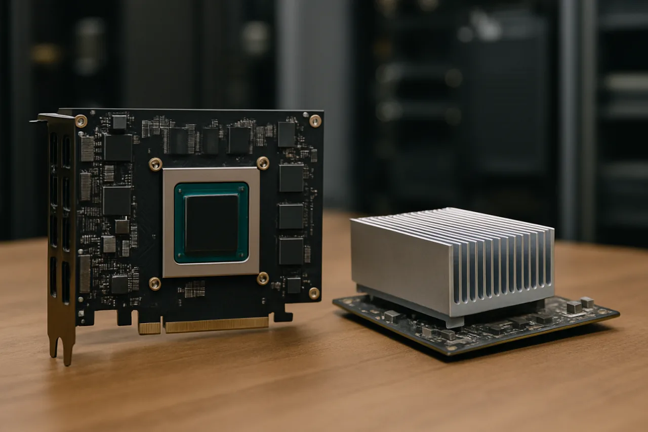
The starting point most comparisons skip: these are not three different species. NVIDIA’s GPUs, Google’s TPUs, and the NPUs shipping inside every AI PC are all variations on one idea — hardware that multiplies matrices in parallel instead of branching through instructions. What separates them is generalism: how much flexibility each design sacrifices to gain efficiency at the workload it was aimed at. Follow that variable through the GPU vs TPU split, and the whole market makes sense.
Why the GPU vs TPU Choice Matters More Now Than Ever
For its first decade, this was a quiet argument. TPUs have powered Google’s search, translate, and assistant workloads since 2015 — designed for internal use, invisible to buyers. GPUs were the generic commodity: programmable, available, expensive. Two things changed in the past 24 months and made the GPU vs TPU question unavoidable.
First, inference became the majority of AI’s workload — and inference is where architecture economics bite hardest. A chip that is 30 percent slower per dollar is tolerable for a one-time training run; across billions of daily queries, it is a permanent margin wound. Google’s own positioning says the quiet part: its seventh-generation TPU, Ironwood, is explicitly marketed as “the first Google TPU designed for the age of inference,” built for “high-volume, low-latency AI inference.”
Second, scarcity did the rest. GPU allocation windows, cloud GPU price hikes, and megawatt-scale campuses made every architect reconsider whether the default answer — rent NVIDIA, everywhere — is actually the cheapest path. The answer increasingly depends on the workload, which is why this comparison now carries real money: compute is the bill, and the chips are the bill’s denominator.
GPU vs TPU: Siblings, Not Twins
The GPU’s defining virtue is programmable generality. A modern data-center GPU is, architecturally, thousands of small cores plus a tensor-core subsystem bolted into the die — originally a graphics processor, now a universal parallel computer. That generality is its moat: CUDA and its ecosystem can absorb a novel architecture (Mixture-of-Experts, sparse attention, speculative decoding) the day the paper ships, without waiting for a hardware revision. It is also NVIDIA’s commercial strategy — the company even spent $3.5 billion in 2026 to make rival chips interoperate with NVLink, widening the ecosystem’s gravity.
The TPU is the opposite bet: a domain-specific machine co-designed with the software that runs on it. Google describes TPU v7 Ironwood as offering 192 GB of memory per chip delivering 7.37 TB/s of bandwidth — figures chosen for the memory-hungry arithmetic of large models rather than shader throughput. The chips connect through high-speed interconnects into pods of up to 9,216 chips treated as a single machine, a topology a GPU cluster traditionally assembles from discrete parts. The TPU’s advantage shows on Google’s home turf: predictable workloads, closed-loop optimization from compiler (XLA) through networking. Its cost is that same specialization — anything outside the supported ops library means losing much of the hardware’s value.
One important honesty note before the numbers: Google states Ironwood delivers 10x the peak performance of its TPU v5p predecessor and more than 4x per-chip performance in training and inference, alongside twice the performance-per-watt of its Trillium generation. Those are vendor claims — as of this writing, no independent party has reproduced them on a named public workload. The claims are plausible (generation-over-generation gains are a repeated Google pattern), but “plausible” and “proven” are different words, and the distinction matters when a procurement decision rides on them.
What an NPU Actually Is — and Why a TPU Is One
The neural processing unit is the most misunderstood of the three. An NPU is a matrix-arithmetic engine built specifically for the operations behind neural networks — and by that definition, Google’s TPU is itself a data-center-scale NPU. What the market means by “NPU,” though, is the chip class shipping in client devices: the dedicated AI engines in Intel Core Ultra (48 TOPS), AMD Ryzen AI (50-55 TOPS), Qualcomm Snapdragon X (45 TOPS, rising past 80 on 2026 models), and Apple’s Neural Engine. Microsoft’s Copilot+ program set the practical floor at 40 TOPS of NPU performance, a spec that effectively redrew the laptop lineup in 2025-2026.
What NPUs buy at client scale is physics, not brute force: sustained AI features — camera effects, transcription, local assistants, small language models — executed at a few watts instead of waking the main GPU. The trade-offs mirror their bigger siblings reversed: an NPU is brilliantly efficient at its supported operators and nearly useless beyond them, which is why local AI today leans on a narrow set of model classes. The gap between peak TOPS and delivered utility is the client-side echo of the same measurement trap that afflicts data-center chips: a 45-TOPS NPU with mature software support routinely beats a 60-TOPS part with thin drivers — execution environment beats synthetic peak.
Here’s the question that matters: if a TPU is an NPU and an NPU is a matrix engine, what stops GPU, TPU, and NPU from collapsing into one product line? Answer: three different masters. The GPU answers to every possible workload; the TPU answers to one company’s software empire; the NPU answers to the battery. Each design is rational for its master, which is why the market keeps all three instead of consolidating.
The Numbers That Matter: Peak Specs vs Delivered Tokens
Vendor spec sheets are a competitive-marketing genre, and this market produces a lot of them. The honest way through: measure what the chips are actually asked to deliver — throughput per unit of cost, power, and time on real workloads — and treat everything else as context.
Raw peak arithmetic: top-tier Blackwell Ultra chips advertise dense FP8 arithmetic around 4.5-5 PFLOPS per GPU at roughly 1,000-1,400 W each, while Ironwood’s peak FP8 rate is similarly classed per chip — near-parity on paper between the two data-center flagships. Peak parity is where the story starts, not ends.
The delivered-work layer: for large-language-model serving, the numbers that matter are tokens per second per rack and per watt. NVIDIA’s own MLPerf Inference submissions claim a GB300 NVL72 rack producing on the order of 674,000 tokens per second on DeepSeek-R1 at the rack’s 132-142 kW draw — vendor-submitted, but produced under MLCommons rules, which makes it citable with the right caveat. On the TPU side, Google leads with systems-of-systems claims (pod-level throughput, 96% reductions in time-to-first-token via its GKE Inference Gateway) that no outside party has replicated.
The independent layer — MLPerf: MLCommons’s training rounds are the only venue where GPU, TPU, and rival accelerators face the same workloads under published rules: the v5.0 round (June 2025) drew 201 results from 20 organizations across 12 distinct processors — AMD Instinct MI300X/MI325X, NVIDIA Blackwell (GB200/B200), and Google’s TPU-Trillium among them. The pattern across rounds is double-edged: NVIDIA’s platform generally takes top-line speed records, TPU pods demonstrate competitive scale efficiency on supported benchmarks, and both sides cherry-pick what they submit. Reading MLPerf like a scientist means reading who submitted what before reading the winner.
The system layer: rack-level engineering decides more than chip-level benchmarks. NVIDIA sells racks, not chips — its GB300 NVL72 pools roughly 20 TB of memory across 72 GPUs in one coherent domain, liquid-cooled and power-hungry. Google sells pods, not chips — 9,216-chip Ironwood enclaves with optical circuit switching. Comparing “a GPU vs a TPU” at the chip level is comparing an engine to a train set; buyers pay for the train.
When Each Architecture Wins: A Buyer’s Decision Map
Synthesis over spec-sheet worship — the practical answer to GPU vs TPU (and where the NPU fits) by situation:
| Who you are | Usually right | Why | The caveat |
|---|---|---|---|
| Developer building on cloud APIs | Neither — model provider’s choice | You buy tokens, not silicon; the provider’s infra pick is priced in | Token price differences (our pricing coverage) reflect exactly this layer |
| Company training/serving own models on cloud | GPU, mostly | Ecosystem depth, portability across clouds, no vendor lock to one stack | Price-compare: TPU instances are frequently cheaper per equivalent token |
| Team serving massive, stable inference at scale | TPU increasingly competitive | Inference-first design, pod efficiency, Anthropic-scale validation (Google names it an anchor customer) | Portability: TPU tooling has narrowed historically; vLLM support is new and maturing |
| Frontier-scale training | GPU ecosystem, today | Every framework lands on CUDA first; multi-cloud flexibility | TPU pods train Google’s own frontier models — the internal proof exists |
| On-device/local AI feature work | NPU, exclusively | Watts: nothing else runs sustained AI at laptop power budgets | Operator support is narrow; test the actual model, not the TOPS figure |
The map’s deeper pattern: the GPU vs TPU axis is increasingly decided by ecosystem maturity per workload, not by silicon. And the edge (NPU) has quietly become the biggest unit-volume market of the three — hundreds of millions of devices shipping yearly, every one of them a small bet on matrix arithmetic without a fan.
The Second-Order Effect: Power Decides the Winner
Zoom out from chips to facilities and the comparison inverts one more level. Every accelerator choice is, at campus scale, a power-systems decision. A Blackwell Ultra GPU drawing ~1,400 W means a standard 72-GPU rack demands 130+ kW — which is why liquid cooling went from exotic to mandatory, and why NVIDIA’s rack architecture now specifies facility water. Google’s answer is a different power curve: Ironwood’s claimed 2x performance-per-watt improvement is precisely an argument that TPU pods deliver more tokens per megawatt — and in a market where interconnection queues decide who builds next, tokens-per-megawatt is a siting advantage, not a marketing line. We covered the infrastructure side of that shift in how AI data center power became AI’s hardest constraint.
The NPU runs the same logic at the opposite pole. A laptop NPU under 5 W is the entire reason local AI features survive a working day unplugged — the client market’s version of tokens-per-watt. Three chips, one shared currency: delivered intelligence per watt. That is the frame the next decade of the GPU vs TPU race will be fought in, from gigawatt campuses to battery life.
What Comes Next: The Boundaries Blur Through 2027
Three watch-lines will redraw this comparison faster than any single spec:
1. NVIDIA entering the laptop. The company has been widely reported collaborating with MediaTek on an Arm-based PC SoC pairing its graphics architecture with high-performance CPU cores — if it ships broadly through 2026-2027, the GPU/NPU boundary in laptops gets re-litigated by the incumbent’s entry, and the Copilot+ TOPS floor becomes a contested marketing line rather than a settled spec.
2. Portability softening the TPU question. vLLM support for TPUs and standardized serving layers reduce the historical switching costs — the closer “GPUs and TPUs as configuration options” gets, The more that convergence lands, the more the GPU vs TPU decision compresses to price-and-efficiency per token, and the more pressure that puts on GPU pricing.
3. Precision convergence. FP8 and FP4 arithmetic have gone from research curiosities to the default serving currencies of both flagship platforms — meaning tomorrow’s comparison will be won on memory bandwidth and interconnect (the data-movement budget) rather than raw FLOPS, favoring whoever integrates memory and packaging best. That is a good reason to read our explainer on data center power and cooling as the other half of this story — heat is arithmetic’s invoice.
The steady prediction: through 2027, no architecture “wins.” The GPU keeps the ecosystem, the TPU keeps the efficiency crown inside Google’s orbit at growing scale, and the NPU quietly becomes the most-shipped AI processor on Earth inside devices nobody calls “AI infrastructure.” The GPU vs TPU debate survives precisely because both keep winning somewhere.
FAQ: What Readers Actually Ask About GPU vs TPU and NPU
GPU vs TPU vs NPU — what is actually the difference?
A GPU is a programmable parallel processor originally built for graphics, now the general-purpose workhorse of AI. A TPU is Google’s purpose-built ASIC for AI arithmetic, co-designed with its own software stack and deployed in multi-thousand-chip pods. An NPU is the device-scale version of the same idea — a matrix engine built for AI features inside phones and laptops. The distinction is scope and control, not fundamental silicon physics.
Is a TPU faster than a GPU?
On peak paper specs, comparable at current generations; in delivered performance, workload-dependent. Google claims Ironwood outperforms its predecessors by multiples and leads on pod-level efficiency — vendor-submitted, independently unverified. Under MLPerf’s neutral rules, NVIDIA platforms generally hold top-line training records while TPU pods show strong supported-workload efficiency. The honest answer: for your workload, benchmark on your model before committing either way.
Can I use a TPU without being Google?
Yes — through Google Cloud, where TPU generations are offered as managed infrastructure, and Anthropic is the most prominent external anchor customer for Ironwood. Third-party serving frameworks like vLLM now support TPUs, and GKE’s inference gateway handles TPU serving at scale. You just should not expect the same ecosystem breadth CUDA offers.
What does TOPS actually mean for NPUs — should I chase the highest number?
TOPS (trillions of operations per second) measures peak theoretical throughput, not delivered utility. A 45-TOPS NPU with mature, native software support often beats a 60-TOPS part with thin drivers — and none of it accelerates cloud-based tools like ChatGPT at all, since those run on servers. Use TOPS as a floor check (40+ for Copilot+ certification), then judge the execution environment.
Do I even need to think about this if I just use ChatGPT or Gemini?
Directly, no — you rent tokens from a provider who made the architecture decision for you. Indirectly, yes: those token prices, latency, and rate limits are downstream of exactly this hardware competition, which is why the GPU vs TPU race shapes what AI costs you, even without a data center of your own.
Which should a startup pick in 2026 — GPU, TPU, or something else?
Default to renting GPUs on the cloud for breadth, benchmark TPU instances against them for stable inference or training workloads where cost per token matters, and reserve NPU work for actual on-device features. Treat every “Xx faster” claim — ours included — as a hypothesis your own benchmark of the GPU vs TPU trade has to confirm before it earns a budget line.
Sources and Further Reading
- Google Cloud Blog — Ironwood TPUs and new Axion-based VMs: cloud.google.com
- Google — Ironwood: the first Google TPU for the age of inference: blog.google
- MLCommons — MLPerf Training v5.0 results (201 results, 20 orgs, 12 processors): mlcommons.org
- MLCommons — MLPerf Training v5.1 results: mlcommons.org
- NVIDIA — MLPerf benchmark resources (GB200/GB300 submissions): nvidia.com
- ModulEdge — NVIDIA GB300 NVL72: specs, power, capacity: moduledge.com
- Qualcomm — Copilot+ / Snapdragon AI performance: qualcomm.com
If this intelligence helps you, you can add WorldNgayon as a preferred source on Google — free, one click, and it helps other readers find the answers faster.