
Table of Contents
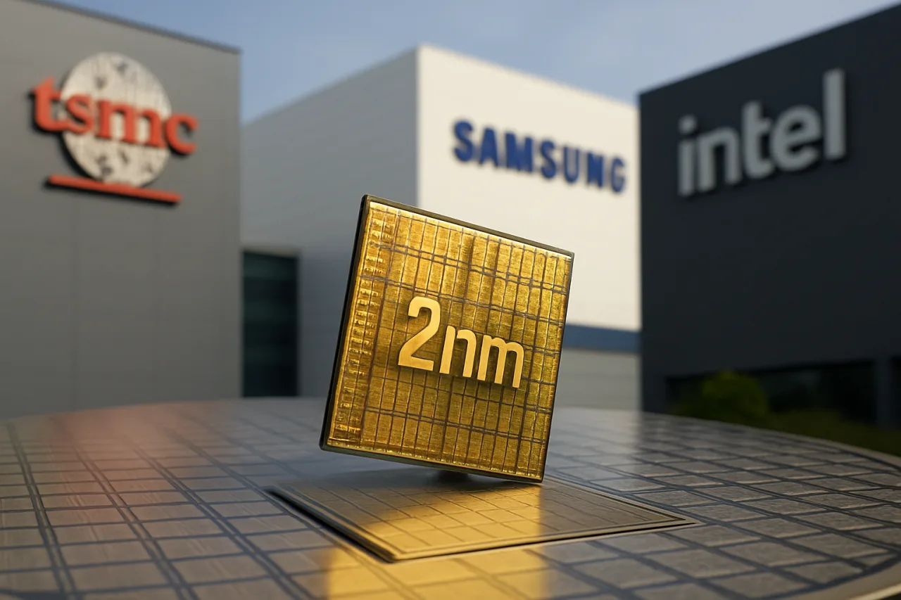
The 2nm chip generation has moved from roadmap to reality — and with it the industry’s first true three-way foundry fight in a decade. TSMC put its N2 process into volume production at two Taiwan fabs in Q4 2025, shipping chips for Apple, Nvidia, AMD and Qualcomm; Intel’s 18A node entered high-volume manufacturing with Panther Lake and a backside-power trick no rival has in a shipping product; Samsung’s SF2 mass production trails on yields near 55% while it undercuts TSMC’s wafers at roughly $20,000. This guide explains what a 2nm chip actually is in plain language, who is winning on verified numbers, what the yield and pricing war means for every device you buy next, and why an Intel high-NA EUV bet in 2027 could redraw the map.
Everything below is dated to the current public record — fab milestones, yield reports and pricing that analysts and trade press have published — with vendor claims labeled as vendor claims until third parties can measure them.
Key Takeaway
- 🥇 TSMC leads the 2nm chip race on execution: N2 entered volume production at two fabs simultaneously in Q4 2025 — the first gate-all-around (GAA) node for the foundry — with Apple, Nvidia, AMD and Qualcomm as the anchor customers and hyperscalers queued behind them.
- 📉 Samsung’s problem is yield, not ambition: SF2 mass production started in 2025 (first into Exynos 2600), but reported yields sit near 55% into early 2026 — below profitable volume — so Samsung is buying share with ~$20,000 wafers, roughly a third cheaper than TSMC.
- 🦾 Intel’s bet is backside power: Intel 18A (an 1.8nm-class node) reached high-volume manufacturing in late 2025 with PowerVia backside power delivery in shipping silicon — plus a High-NA EUV lithography ramp planned for 2027-28, years ahead of rivals.
- 💰 Foundry economics are top-heavy: TSMC’s quarterly foundry revenue runs roughly 11 times Samsung’s foundry unit ($35.9B vs $3.2B in Q1 2026) — scale, not node names, is the moat.
- 🇵🇭 What it means for Filipino buyers and workers: the 2nm generation lands first in phones and laptops (Philippine consumers buy these nodes through global brands) and lands again in regional assembly and test work — the semiconductor skills lane our AI-proof careers analysis tracks.
What a 2nm chip actually means (plain-language)
The nanometer stopped being a literal measurement years ago — a “2nm chip” is a marketing class label for the newest gate-all-around (GAA) transistor generation, in which the transistor’s gate wraps the current-carrying channel on all four sides, replacing the fin-shaped (FinFET) transistors every node since 22nm used. The wrap improves control of the current, which means the same work needs less power — or more speed at the same power. What actually changes between nodes is measurable in three numbers per foundry: power (TSMC’s N2 runs 25-30% lower than N3E at equal speed), performance (+8-15% at equal power depending on flavor) and density (about 1.1-1.23x by node variant).
Two truths matter more than the marketing. First, TSMC’s N2 lacks backside power delivery — the analyst note behind the “mediocre density gain” verdict versus N3E — so the node’s headline is power efficiency, not density. Second, backside power (routing the power rails to the wafer’s underside) is the industry’s next structural step: Intel ships it first (PowerVia inside 18A), Samsung’s SF2Z brings it in 2027, and TSMC’s A16 adds it in the generation after N2. A 2nm chip without backside power is the current frontier; a 2nm-class chip WITH backside power is the next one.
The 2nm chip scoreboard: the three foundries on verified numbers
| Foundry | Node | Status (verified date) | Yield / pricing | Anchor customers |
|---|---|---|---|---|
| TSMC | N2 (GAA nanosheet) | Volume production Q4 2025 at two Taiwan fabs | Premium pricing; N2P + A16 (backside power) roadmap; A14 in 2028, re-skinned for data centers 2029 | Apple, Nvidia, AMD, Qualcomm; hyperscalers (Microsoft, Amazon, Google) named by analysts |
| Intel | Intel 18A (1.8nm-class, GAA + PowerVia) | High-volume manufacturing late 2025 (Fab 52, Arizona) | Panther Lake and Clearwater Forest shipping internal; external foundry customers being courted | Intel products first; external wins pending credibility-building |
| Samsung | SF2 (GAA) → SF2P → SF2X → SF2Z | Mass production since 2025 (Exynos 2600); Taylor, Texas fab equipped in April 2026 | Yields ~55% into early 2026; 2nm wafer price cut to ~$20,000 — about 33% below TSMC | Tesla’s AI6 on an eight-year $16.5B deal (reportedly slipped ~6 months) |
The gap behind the leaders is revenue, measured: TrendForce put TSMC at $35.86 billion of foundry revenue in Q1 2026 against Samsung’s ~$3.2 billion — an 11:1 gap — analysts’ shorthand “second by a factor of ten.” Intel’s foundry is still climbing toward external relevance. The 2nm chip race is therefore run in three lanes at once: engineering (who ships the transistor first), economics (who prints it profitably) and geopolitics (who else can print it at all) — the geopolitical lane our China-US AI race analysis and the EUV lithography explainer (the $200M machines beneath every node) cover in depth.
The yield war behind the 2nm headlines
Yield — the percentage of good dies from a wafer — decides who profits at scale, and it is the 2nm chip race’s real yield problem, and the verified reports agree on the shape: TSMC executes its roadmap on schedule and predictably (two fabs of N2 at once, a first in recent memory), Samsung struggles (first-generation 2nm yields reported near 55% into early 2026, prompting reports that Qualcomm could route work back to TSMC, and a delayed engineering run that slipped Tesla’s AI6 toward late 2027), and Intel is proving out PowerVia in production before courting the big external names. Samsung’s answer is price: cutting 2nm wafers to around $20,000 — roughly a third below TSMC — while running sub-break-even yields, a combination only sustainable because Samsung’s foundry sits inside a division with a record-profit memory business subsidizing the runway (the memory side of that house runs the HBM shortage calculus).
The practical read for buyers: the yield problem, not the node name, sets your device’s maker — TSMC’s N2 gets the premium devices first (Apple’s class), Intel’s 18A gets the PC first (Panther Lake), and Samsung’s SF2 competes on price for volume-sensitive designs — which is why the 2nm chip in YOUR next phone may be a TSMC part while your next mid-range device may ride a Samsung-priced node.
The roadmap beyond 2nm: who gets to 1.4nm first
| Node | TSMC | Intel | Samsung |
|---|---|---|---|
| 2nm-class + backside power | A16 (adds BSPDN to N2P base) | 18A ships with PowerVia already | SF2Z in 2027 |
| 1.4nm-class | A14 in 2028; data-center version with BSPDN 2029 | 14A next; High-NA EUV ramp 2027-28 | SF1.4 — now officially 2029 (delayed from 2027) |
| Lithography edge | Standard EUV (per TSMC’s predictable roadmap) | High-NA EUV first (2027-28) | Standard EUV; pellicle decision pending |
The lithography row is the sleeper: Intel buys High-NA EUV years ahead of the others, betting that the machine generation becomes a lead; TSMC is the high-volume incumbent with the largest fleet; Samsung’s 1.4nm slipped to 2029, which removes it from the shortest-lead contest. Rapidus (the Japanese entrant) targets the same frontier — a fourth lane worth watching, though with production years behind the leaders.
What the 2nm chip race means for phones, laptops and data centers
Phones and laptops first: the node’s power-efficiency gains show up as battery life and sustained performance before anything else — TSMC’s N2 lands in Apple’s class first, Samsung’s SF2 already runs the Exynos 2600, and Intel’s 18A targets the PC through Panther Lake. Data centers second: the same efficiency math is why hyperscalers queue for N2-era capacity — every percentage point of power saved per transistor scales into megawatts saved per campus (the constraint ladder our power pipeline and sovereign AI pieces track). The risk, stated plainly: leading-edge capacity concentration — one island printing most of the world’s most advanced chips — is the geopolitical exposure analysts name first, which is exactly why the US CHIPS spending and Japan’s Rapidus exist as hedge plays.
WorldNgayon Insight: what the yield reports are really saying
What changed: the 2nm chip generation is the first with three credible foundry strategies since Intel’s old dominance — execute (TSMC), disrupt (Intel’s backside power + High-NA bet), and buy time (Samsung’s price cut). Why now: GAA transition physics, AI’s power budget and export-control politics all landed in the same window. Why it lasts beyond the news cycle: the roadmap row above runs to 2029 with named update triggers — every quarterly yield report, the Tesla AI6 slip, High-NA EUV shipments and the A14/A16 milestones. Who is affected: phone and PC buyers get the efficiency first; hyperscalers get the power math second; the foundry labor market gets the hiring wave third. What to do next: treat “2nm” on a product box as a class label and check the fab behind it — the same spec name hides three different process realities. Risks, opportunities, costs, skills: the risk is supply concentration; the opportunity is the yield-war pricing for mid-range designs; the cost is the largest capex race in semiconductors; the skill shortage runs through process, test and assembly engineering — the lane the Philippines’ own semiconductor workforce occupies. Connection to work and money: the foundry race is also a jobs map — process engineers, test technicians and reliability specialists are the humans behind the yields, and the demand follows the fabs.
For Filipino readers: the node race’s local footprint
The Philippines is a semiconductor export economy — one of Asia’s largest by export value in the test-and-assembly tier — and the 2nm chip generation touches that workforce twice. First, the devices Filipino consumers buy in 2026-2027 (flagships with N2-class chipsets, laptops with 18A-era processors) carry the power-efficiency gains this race produces; the “which chip is in my phone” question is becoming a fab question. Second, the regional industry that packages, tests and supports these nodes — the Philippine Economic Zone electronics corridor — competes for that work against Vietnam, Malaysia and Taiwan’s ecosystem, and advanced packaging growth (the same structural demand behind the HBM memory shortage) raises value for skilled test and packaging labor. The honest frame: the front-end wafer is a three-company race; the back-end jobs map is wider, and Filipino workers already hold a piece of it.
What does 2nm chip mean in simple terms?
A “2nm chip” is the newest class of transistors (gate-all-around, replacing fin-shaped ones) that wraps the gate fully around the channel for better current control — meaning the same work at lower power, or more speed at the same power. The name is a class label, not a physical measurement; what matters is the measured power, performance and density gains per node.
Who makes 2nm chips?
Three foundries as of this date: TSMC (N2, volume production Q4 2025 at two Taiwan fabs — customers include Apple, Nvidia, AMD and Qualcomm), Intel (18A, an 1.8nm-class GAA node with backside power delivery, in high-volume manufacturing since late 2025), and Samsung (SF2 GAA, in mass production since 2025, first into Exynos 2600, with reported yields near 55% into early 2026). Japan’s Rapidus is the named fourth entrant, years behind on production.
Which company is winning the 2nm race?
On execution and economics: TSMC — volume production at two fabs simultaneously, premium customers, and a quarterly foundry revenue lead of roughly 11:1 over Samsung’s foundry unit ($35.9B vs $3.2B in Q1 2026 per TrendForce). Samsung competes on price (~$20,000 wafers, about a third below TSMC) with sub-target yields; Intel’s 18A leads on backside power and holds the High-NA EUV card for 2027-28.
Is a 2nm chip better than 3nm?
By the foundries’ published targets: yes on power — TSMC’s N2 runs 25-30% lower power than N3E at equal speed with 8-15% more performance depending on variant. Independent verification comes from shipping products rather than slides, so treat the deltas as roadmap claims until device reviews measure them; the honest note is that N2’s density gain over N3E is described by analysts as modest, and TSMC’s next node (A16) adds backside power delivery for the bigger step.
What chips use 2nm technology?
First wave (2025-2026): flagship phone SoCs (Apple-class designs on N2; Samsung’s Exynos 2600 on SF2), PC processors (Intel’s Panther Lake on 18A), and server-bound designs including AMD’s EPYC Venice-class CPUs on N2 — with hyperscaler custom silicon named by analysts as the queued customer class. AI accelerators arrive as capacity frees from the phone ramp.
Why are Samsung’s 2nm yields low?
GAA yields in first-generation production are hard for every foundry, and Samsung’s first-gen SF2 ramp landed with reported yields near 55% into early 2026 — below the level for profitable volume at premium pricing — which is why Samsung cut wafer prices and reports say Qualcomm could route work back to TSMC; the company targets SF2P and later variants for the yield recovery.
What is backside power delivery?
Routing the chip’s power rails to the wafer’s underside instead of fabricating them in the wiring layers alongside signals — it frees front-side wiring for data, reduces power losses and improves performance in dense chips. Intel ships it first in production (PowerVia in 18A), Samsung brings it in SF2Z (2027), TSMC in A16 after N2. It is the structural step that follows the GAA transition.
Does the 2nm chip matter for AI?
Directly: AI accelerators and data-center CPUs are the largest single power consumers in the buildout, and node-level efficiency converts into megawatts saved per campus — the reason hyperscalers are named among N2’s next customers. The node race is quietly an energy race, and the factories that print it are the chokepoint covered in our EUV lithography explainer.
Sources: Wikipedia — 2 nm process (node timeline, verified entry points). Additional context cited without links (paywalled or unstable endpoints in this environment): EE Times analyst survey (TSMC to lead rivals at 2nm; N2 customers and the “mediocre density gain” note); Tom’s Hardware — leading-edge foundry roadmaps and the yield-and-pricing war (Samsung ~55% yields, $20,000 wafers, Tesla AI6 slip, Intel High-NA EUV 2027-28, A14/A16 roadmap); TrendForce quarterly foundry revenue (Q1 2026, $35.86B vs ~$3.2B). Vendor benchmark claims are labeled as vendor/analytics claims until measured in shipped products.