
EUV lithography explained in plain terms: it is the machine layer that prints every AI chip you have heard of — the GPUs that power model training, the TPUs, the memory dies beside them — and the machines do it with light so short (13.5 nanometers) that generating it means firing a laser at 50,000 tin droplets per second to create a plasma brighter than the sun’s surface. There is exactly one company that builds them: ASML, of the Netherlands, charging around $200 million per standard machine and up to $400 million for the newest High-NA versions — 400,000 pounds of instrument that flies to a chip fab in three Boeing 747s. This guide explains, without the jargon wall, how the technology works, why a decade of attempts made Nikon and Canon quit instead of compete, why the price is going up — not down — and why even the US government’s chip agenda runs through one building in Veldhoven.
Key Takeaway
- 🖨️ The machine: EUV lithography prints the smallest features on every advanced chip with 13.5-nm light — made by vaporizing tin droplets with a laser, 50,000 times a second, into a plasma that emits the light.
- 💸 The price: roughly $200 million per standard EUV system, up to $400 million for High-NA (the 2nm-class frontier); the mass-production model landed at $100 million in 2017 (ASML’s own EUV product pages document the systems) and the price only climbs.
- 🏢 The monopoly: one supplier — ASML; its mirrors come from Zeiss at sub-nanometer precision, the machine carries over 100,000 modules from ~800 suppliers, and Nikon and Canon abandoned the race.
- 📈 The AI effect: EUV systems went from 46% to 66% of ASML’s quarterly sales inside a year as AI demand devoured the fab calendar — 48 EUV systems shipped in 2025, 60 planned for 2026, 80 a year planned for the future.
- 🛰️ The geopolitics: export controls collapsed China’s share of ASML’s sales from 49% to 19% — while the EUV share of sales grew, proving where the world’s chip budget is going.
What EUV lithography is — in plain language
Every advanced chip starts as a wafer of silicon onto which a machine prints transistors — the on/off switches that do the computing — a layer at a time. The printing machine is called a lithography system, and the printing light decides how small the features can be: shorter wavelengths draw finer lines, and finer lines mean more transistors on the same wafer. That is the whole industry in one sentence, and it is why lithography sits where it does: the light is the limit. For decades the industry marched from mercury-vapor ultraviolet (365 nm) to deep ultraviolet (DUV), squeezing feature sizes down step by step. Then the physics demanded a leap: features below what DUV light can draw cleanly.
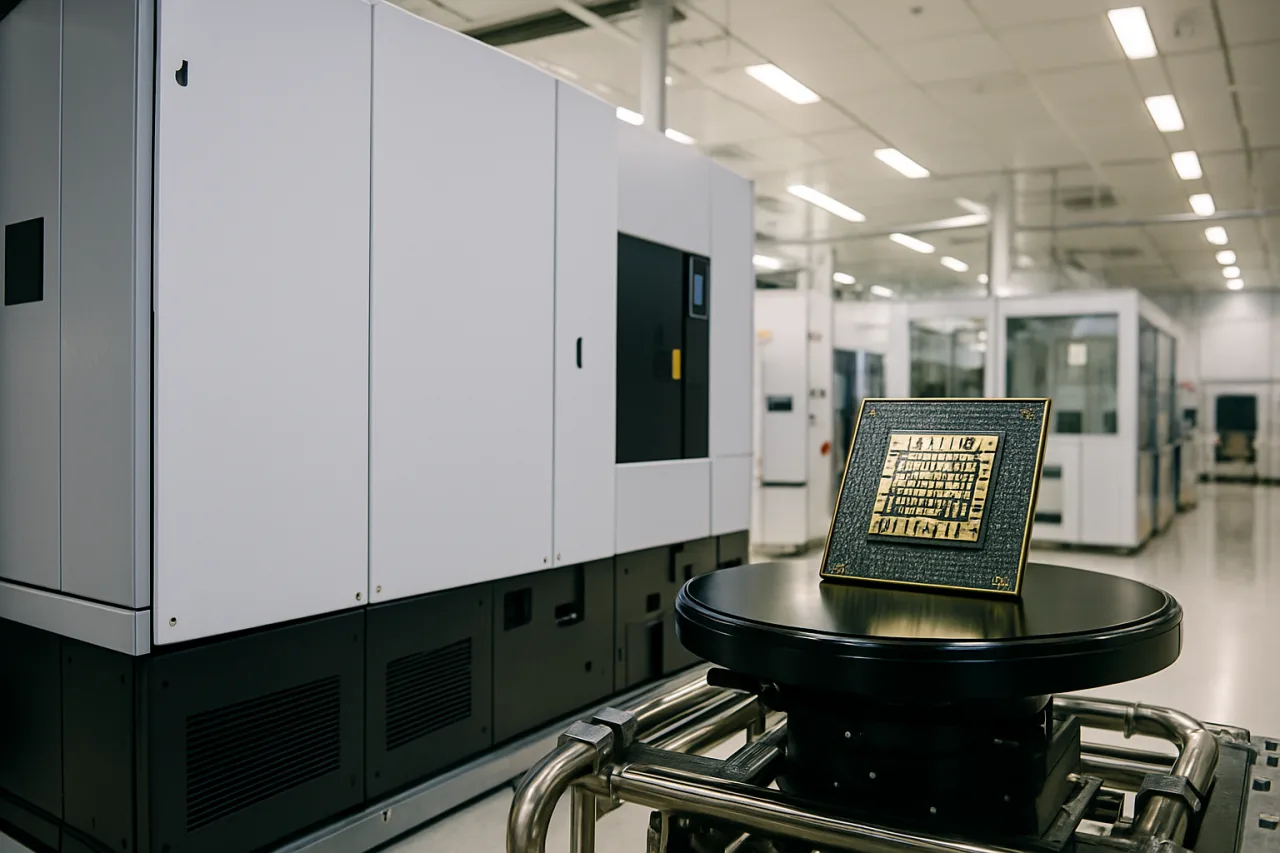
EUV lithography — extreme ultraviolet printing — is that leap: light at 13.5 nanometers, nearly 30× shorter than the original ultraviolet era. But 13.5-nm light is awkward: it is absorbed by practically everything, including air and glass lenses. So the EUV system runs in vacuum, bounces its light off multilayered super-mirrors instead of through lenses — mirrors polished by Zeiss to shape errors smaller than a single nanometer, often described as smooth to the scale where, enlarged to the size of a country, the tallest bump would be a millimeter tall — and generates the light itself by an industrial absurdity that works: a laser fires into a river of molten tin droplets falling at 50,000 per second, each droplet vaporized into a plasma that radiates the 13.5-nm light. The plasma light bounces through the mirror train, through the mask stencil of the chip’s layer, and prints the pattern onto a photoresist-coated wafer — the wafer stepping 220 times an hour through the machine’s heart. Every generation since 2018’s first EUV high-volume production has sharpened this dance; the physics did not change, the engineering multiplied.
The lineage of EUV lithography is older than the AI era. A Japanese researcher, Hiroo Kinoshita, demonstrated EUV imaging from Japan’s NTT lab back in 1985-86, adapting mirror research of Soviet origin — a presentation met with skepticism that seeded three decades of development. The commercial race then ran through the 1990s consolidation (when Nikon and Canon overtook America’s GCA) to the 2010s: ASML shipped EUV prototypes in 2010, hit a commercially viable system by 2013, and mass-production-grade machines at $100 million apiece by 2017 — the point where Intel, TSMC and Samsung decided the printing monopoly priced in.
Why only ASML builds the EUV lithography machine
The honest answer combines physics, economics and a supply-chain empire. The physics: the EUV lithography system is less a machine than a networked city — the tin-plasma light source by Cymer (an ASML acquisition), the miracle mirrors by Zeiss, the wafer stages that move at high speed with nanometer accuracy, thousands of sensors calibrating alignment in real time — over 100,000 modules from around 800 suppliers, each module the product of its own deep supply chain. ASML outsources about 90% of its modules and runs the company as the R&D leader and system integrator of the whole stack. The economics: EUV is a decades-long compounding of capital and learning curves — Nikon and Canon, the industry’s former giants, both abandoned EUV rather than fund the climb; the incumbent makers of DUV simply priced themselves out of entering a $10-billion-class R&D tunnel with one guaranteed buyer-base. And the strategy: instead of building EUV in-house, Intel, TSMC and Samsung INVESTED in ASML — the customers own stakes in the sole supplier, a structure with no real precedent in heavy industry.
The result: an effective monopoly ASML holds with roughly 90% of all lithography tools sold, and 100% of EUV. A recent Communications of the ACM monograph — the most complete public anatomy of the empire — reads it plainly: the platform-ecosystem leadership model is what makes the machine uncopiable; the Chinese state’s “Manhattan Project” response runs a decade-plus behind and, per its own published roadmap, has not shipped a production EUV equivalent.
The price tag: $100 million to $400 million per machine
The numbers, plain: mass-production EUV machines landed at about $100 million in 2017. Today’s standard EUV lithography systems — the NXE generation — run around $200 million for the less sophisticated configurations, and the High-NA frontier machines approach $400 million for the 2nm-and-denser node work. The physical reality matches the invoice: each system weighs about 400,000 pounds, ships in 40 freight containers’ worth of parts, and needs three chartered Boeing 747s — the largest cargo flights in industry. Installation into a fab takes months. In 2025 ASML shipped 48 EUV systems out of 327 lithography machines of all types — the industry’s own capacity tracking shows tool supply stretching against AI demand — the EUV fleet is the smallest, most expensive slice of a tool market it alone serves; the plan books show 60 EUV systems for 2026 and — for the coming years — 80 per year. Every machine sold is a decade of guaranteed use inside the fabs’ own roadmaps: the customers pre-book years ahead because the alternative is not a rival vendor; it is no second source at all.
The pricing’s honest context: the price climbs because each generation buys a smaller feature with lower defect rates and higher throughput — the machines print MORE wafers per hour on finer nodes, which is what keeps Moore’s Law’s economics on the right side of physics. The bill of goods is not one machine; it is the wafer’s cost curve: EUV layers on a 2nm-class chip are the most expensive steps in the fab — the memory side squeezes alongside it (DRAM contract prices climbing again in Q2 per the supply-chain trackers) — which brings the story to the AI connection.
The AI-chip connection: 46% to 66%
Why does an explainer about printing machines sit on an AI-infrastructure pillar? Because the AI demand surge re-priced the whole tool-market, and the receipts sit in ASML’s own quarterly books. In Q1 2026, EUV systems were 46% of ASML’s sales; a quarter later, as the High-NA era began ramping and China’s export-controlled share collapsed, the EUV slice of sales had grown to 66%. The buyers are the companies training and deploying AI: TSMC’s N2-class lines for the next Apple and Nvidia silicon, Intel’s 18A return to competitive manufacturing, Samsung’s memory-and-foundry stack — every H100-class GPU, every Blackwell successor, every TPU and accelerator printed in those fabs passes through EUV layers, and the memory chips beside them (the HBM shortage our guide covers) ride the same tooling. The quarterly receipts: Q3 2026 net sales €11.7 billion with €5.0 billion net income, full-year 2026 guided to €44-45 billion — numbers that grew not despite the AI boom but from its fab calendar.
The AI infrastructure stack runs: light (the laser-plasma) → the wafer layers (EUV) → the accelerators and HBM (Nvidia and the memory trio) → the racks and cooling (our power guide and the water-wall piece) → the models you use. Read ASML as the first meter of that chain — the layer whose physics the rest inherits.
Export controls: how a machine became geopolitics
EUV lithography became a border because of what the machines enable. Under US-Dutch export-control coordination, the most advanced EUV and High-NA systems cannot be shipped to China — the collapse in ASML’s China percentage (49% of sales to 19% across quarters) is the policy writing itself into commerce. The counter-move: China’s domestic lithography program — the effort our PH-adjacent fab guide tracks regionally — the “Manhattan Project” of chip-making — funds DUV multipatterning workarounds and its own EUV prototype research, with published roadmaps that trail by years, not quarters. The pattern to hold onto: wherever the machine is, the AI chip supply is; and wherever the machine is denied, the chips above it get harder to build. This is why the AI race’s map (our China-vs-US explainer) has lithography as one of its core provinces.
The 2030 path: why light power is chip price
The next decade’s dial in EUV lithography is light power. Today’s EUV source runs at about 600 watts; the announced roadmap — 1,000 watts by 2030 — doubles wafer throughput toward ~330 wafers per hour, up from about 220 today, which translates directly into cheaper cost per chip: more wafers per machine-hour amortize the $200-400M invoice across more silicon. The physics plan reads like science fiction with a shipment date: lasers firing 100,000 tin droplets per second (double today’s rate) shaped by two laser bursts instead of one — and ASML’s own light-source technologist states the path continues: 1,500 watts within reach, 2,000 watts with no fundamental blocker. The honest caveat, from the same reporting: the 1,000W class stays years from commercialization, and the interim throughput gains ride process tuning. The strategic read for the pillar: throughput is where EUV’s next cost curve bends — and it is the one ASML controls alone.
What it means for the prices you pay
The machine’s invoice travels down the stack into every device price. A fab’s EUV lithography bill is a fixed cost per wafer; when wafers carry EUV layers, the wafer’s price floor sits higher — and the chips that matter for AI (GPUs, accelerators, HBM stacks whose shortage our guide covers) carry the most EUV layers of all. The consumer receipts stack on top: this year’s AI-driven memory crunch has escalated everything from GPUs (retail RTX 5090s trading at multiples of MSRP, the flagship’s production constrained) to consoles and hand-helds — because every chip in the family inherits fab costs and the memory market’s squeeze. The practical layer the reader can act on: AI-capable consumer hardware prices climb while EUV-era capacity tightens — the buying calendar matters, and the infrastructure stories upstream (the power grid, the water wall, the lithography queue) are the leading indicators of when relief comes. A reader who understands the first meter of the chain understands the whole bill.
For the chips’ consumer side — the HBM memory shortage, the GPU-vs-TPU-vs-NPU anatomy, and the price spikes on retail shelves — our pillar guides cover those layers; this explainer completes the stack’s foundation.
FAQ
What is EUV lithography in simple terms?
It is the printing process that draws the smallest transistor patterns on advanced chips using extreme ultraviolet light at 13.5 nanometers. The light is created by firing lasers at molten tin droplets 50,000 times a second, producing a plasma that emits the short-wavelength light, which bounces off near-perfect mirrors to print the chip’s circuit layer.
Why do EUV machines cost $200 million?
The mirrors are polished to sub-nanometer precision, the machine integrates over 100,000 modules from ~800 suppliers, and each generation must print finer features with higher throughput on denser nodes. The High-NA frontier versions approach $400 million. Price follows the physics: the machine is the only way to print 2nm-class chips.
Does any company other than ASML make EUV lithography machines?
No. ASML is the sole producer of EUV lithography systems (and roughly 90% of lithography tools overall). Nikon and Canon abandoned the EUV race; Intel, TSMC and Samsung invest in ASML as customers; China’s domestic program funds prototype work but has not shipped a production EUV equivalent.
Can China buy EUV machines?
No — under US-Dutch export controls, the most advanced systems cannot be shipped to China; ASML’s China revenue share collapsed from 49% to 19% across quarters as controls tightened. China funds its own lithography development, which trails on EUV-class printing.
How is ASML and EUV lithography connected to AI chips?
Every advanced GPU, AI accelerator and HBM memory stack is printed, layer by layer, with EUV lithography inside fabs owned by TSMC, Intel and Samsung. The AI boom’s demand re-priced the tool market: EUV systems went from 46% to 66% of ASML’s quarterly sales, and 2026 shipments plan 60 EUV systems against 48 in 2025.
Will EUV machines ever get cheaper or faster?
Both — different directions. Throughput improves: the roadmap targets 1,000W light sources by 2030 (about 330 wafers/hour vs 220 today), which lowers cost per chip, with a 1,500-2,000W path beyond. Feature costs per generation still climb: High-NA machines at $400 million print finer nodes, and the industry’s wafer bills climb until the next capacity wave lifts supply.
Related reading: the sovereign AI scoreboard these machines gate.