
Table of Contents
Key Takeaway
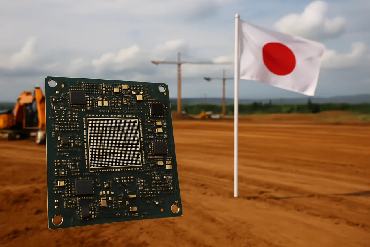
- 🏭 The confirmed signal: an unnamed Japanese semiconductor facility is planned for a 20-hectare manufacturing site at LIMA Estate in Batangas, with groundbreaking intended for November 2026, Aboitiz CEO Rafael Fernandez de Mesa said.
- 🔒 The important limit: the company, investment value, product line, hiring target, production date, and PEZA registration status have not been publicly identified in the announcement reviewed for this article.
- 🧩 The strategic meaning: the project would be an expansion by a company already operating somewhere in the Philippines—not proof, yet, of a new wafer fab or an advanced-chip plant.
- ⚡ The execution test: the project must move through company disclosure, PEZA registration, permits, construction, utilities, equipment installation, hiring, and production qualification before it becomes operating capacity.
The planned Japanese semiconductor facility at LIMA Estate is more than a 20-hectare land announcement, but it is also less than a confirmed operating factory. The first distinction matters because semiconductor projects are often described as “plants” before the public knows whether they will perform wafer fabrication, packaging, testing, component production, or another part of the electronics value chain. The second distinction matters because the project’s company name, capital expenditure, product scope, employment target, and production timetable remain undisclosed.
What is known is still significant: Aboitiz Economic Estates says a large Japanese semiconductor company already present in the Philippines intends to add a second location at its LIMA Estate in Batangas, with a groundbreaking planned for November 2026. That puts the proposal inside an established industrial ecosystem rather than an empty site. It also gives WorldNgayon readers a more useful question than “Who is the mystery company?”: what evidence will show whether the Japanese semiconductor facility becomes real industrial capacity?
What the Japanese Semiconductor Facility Announcement Confirms
The Philippine Star reported on October 4 that Rafael Fernandez de Mesa, Aboitiz Economic Estates’ chief executive, told reporters about the project. He characterized the investor as a major Japanese global company, but did not name it. The report identified four concrete details:
- The investor is a Japanese semiconductor firm.
- The company already runs a separate industrial operation in the Philippines.
- The new site is inside LIMA Estate in Batangas.
- The planned property covers 20 hectares, with groundbreaking targeted for November 2026.
Those facts establish an expansion plan, not an operating facility. The phrase “plans to break ground” describes an intended construction milestone. It does not establish that construction has started, that the site has received every approval, or that the building will produce components by a particular date. The Philstar report also did not disclose the project’s investment value, expected workforce, manufacturing technology, or first production date.
This is the point at which many industrial stories become less accurate. A large site can support a large factory, but land area alone cannot identify the factory’s process. The Japanese semiconductor facility should therefore be reported as a planned expansion with a scheduled groundbreaking—not as a completed investment or a new fabrication plant.
Why the Japanese Semiconductor Facility Matters Without a Company Name
The missing company name limits what can responsibly be said, but it does not erase the signal. An established semiconductor operator choosing another Philippine location suggests that the country’s industrial ecosystem may be supporting additional capacity decisions from companies already familiar with its workforce, suppliers, regulations, logistics, and operating costs.
De Mesa said approximately half of Aboitiz Economic Estates’ new locators each year come either from its own Philippine network or from companies already operating in the country that are expanding inside its industrial estates. That observation is not a measurement of the Japanese project itself, and it does not prove that every existing locator is satisfied. It does point to a pattern worth tracking: repeat investment can be a stronger confidence signal than a one-time expression of interest because the investor has already experienced the operating environment.
The distinction is important for readers who follow industrial policy. A new entrant must evaluate the Philippines from outside. An expansion decision is made by a company with existing local knowledge. It may still be driven by incentives, customer demand, export orders, or a global reorganization of production, but it is not based only on a promotional roadshow.
That is why the Japanese semiconductor facility belongs in the country’s industrial construction pipeline even before its company name is public. It adds a possible expansion by an existing player to a sector already under pressure to increase output, attract higher-value activities, and develop specialized talent.
What the 20-Hectare Site Does—and Does Not—Tell Us
Twenty hectares is a substantial industrial footprint. It can accommodate production buildings, utilities, loading and storage areas, internal roads, support facilities, employee services, and room for phased expansion. For a semiconductor or electronics operator, that flexibility can matter as much as the first building: manufacturing layouts often require controlled environments, specialized power, water and wastewater systems, chemical handling, testing areas, and carefully managed logistics.
But the number does not reveal the technology. Semiconductor production is a chain rather than a single activity:
- Front-end fabrication creates transistor structures on silicon wafers and requires extremely expensive cleanroom, lithography, process-control, and utility systems.
- Back-end assembly, packaging, and testing turns manufactured dies into usable components and verifies their performance. These operations can still be highly technical and capital-intensive without being wafer fabs.
- Component and module production combines semiconductor devices with sensors, boards, connectors, optics, power electronics, or other parts for automotive, industrial, consumer, or communications products.
The announcement does not say which of these activities the Japanese semiconductor facility will perform. Calling it a “chip fab,” an “AI-chip plant,” or an “advanced-packaging campus” would add facts that have not been disclosed. The correct editorial position is to leave the process open until the company or regulators identify it.
That restraint does not make the story smaller. It makes the next update more valuable. Once the company discloses its process, WorldNgayon can assess what the project contributes to the Philippines: production volume, technology transfer, supplier demand, energy and water requirements, workforce needs, and the country’s position in the regional value chain.
LIMA Estate Gives the Project an Operating Base
LIMA Estate is not a greenfield concept waiting for its first tenant. Aboitiz Economic Estates describes the Lipa-Malvar development as a 1,100-hectare industrial-anchored estate with more than 200 companies, approximately 75,000 jobs, and more than ₱128.9 billion in cumulative investment. Those figures are the estate operator’s published figures and should be read with their stated dates and definitions, but they show why a manufacturer might choose an established site.
Marubeni’s profile of Lima Technology Center, updated with information stated as of June 2025, describes a PEZA-accredited industrial park with access to the Manila and Batangas ports, a 69-kilovolt power grid with a stated 150 MVA supply capacity, 14,000 cubic meters per day of water supply, and centralized wastewater treatment. The same profile lists around 200 operating companies at that point. The different dates explain why published locator and workforce counts should not be mixed as though they were measured on the same day.
For a semiconductor operator, this infrastructure is not decorative. Power quality, water availability, wastewater treatment, customs procedures, roads, fiber connectivity, worker transport, and supplier proximity all influence whether a site can move from construction to reliable production. The Marubeni Lima Technology Center profile also lists Japanese-linked companies among the park’s locators, including electronics, precision, automotive, and materials-related businesses. It does not identify the new investor, but it helps explain the kind of ecosystem the company would be joining.
Aboitiz’s own account emphasizes a similar model: industrial land is paired with power, water, construction, digital connectivity, housing, education, and talent initiatives. That integrated structure can reduce the number of separate site decisions an incoming or expanding manufacturer must make. It cannot eliminate construction, regulatory, or market risk, but it can shorten the distance between a land reservation and an operational plan.
How the Project Fits the Philippines’ Semiconductor Push
The proposed Japanese semiconductor facility arrives while the Philippine government is trying to move the country’s electronics sector beyond its traditional strengths. The Department of Trade and Industry’s Philippine Semiconductor and Electronics Industry Roadmap targets $110 billion in annual exports by 2030: $70 billion from semiconductors and $40 billion from other electronics. The DTI also says the roadmap includes up to three national laboratories, each with specialized fabrication capability, research and development plans, and talent-development work.
The national roadmap is an industrial strategy. The LIMA project is a private-sector site decision. The Japanese semiconductor facility is one possible physical test of whether that strategy attracts new capacity. They should not be treated as the same thing. The project does not prove that the roadmap target will be achieved, and the roadmap does not prove that this specific facility will receive public funding or produce a particular class of chip.
They are connected, however, because the roadmap needs actual factories, suppliers, laboratories, utilities, and workers. A planned expansion by an existing semiconductor operator is one of the concrete projects that can test whether policy ambition is becoming industrial capacity. Our broader Philippine semiconductor industry analysis covers the national value-chain goal; this story adds a site-level question: where will that capacity physically be built?
The project also sits within a wider effort to strengthen trusted supply chains. The United States and the Philippines announced plans in April 2026 for a proposed 4,000-acre economic-security zone under the Pax Silica framework. The official announcement describes semiconductors, electronics, critical minerals, and advanced manufacturing as relevant supply-chain areas. That does not place the LIMA project inside the proposed hub, and no source reviewed for this article says that it is a Pax Silica tenant. The more careful reading is that the project benefits from a broader policy environment in which allied governments are trying to diversify critical-technology production.
The Real Constraint Is Not the Groundbreaking Ceremony
Groundbreaking is visible. Utilities and talent are less visible, but they determine whether a facility becomes productive. De Mesa told reporters that the country must be ready not only with land, but also with utilities and a talent pool. That is the central execution test for this project and for the Philippines’ larger semiconductor ambitions.
A semiconductor facility can require specialized electrical systems, stable water and wastewater services, environmental controls, cleanroom technicians, equipment engineers, quality specialists, process personnel, logistics teams, and managers who understand customer qualification. If the project is focused on packaging or testing, its needs will differ from those of wafer fabrication. That is another reason not to invent a workforce number before the company identifies its process.
Permitting is another milestone. Aboitiz and the Philippine Economic Zone Authority are also working on the next phase of EaseBiz to support locator registration and operations. In the same report, PEZA chief Tereso Panga said 80% of the agency’s permitting processes had been automated and that full automation was targeted for the following year. Faster processing can reduce administrative friction, but it is not the same as approval of this specific facility. Readers should look for a PEZA registration or project announcement tied to the company by name.
The useful sequence is therefore straightforward: identify the investor; confirm the site and project scope; verify PEZA and other regulatory milestones; confirm construction; establish the facility’s technology and investment value; then track hiring, equipment installation, qualification, and production. Each step converts a general announcement into evidence.
What the Japanese Semiconductor Facility Could Mean for Workers and Suppliers
No job target was announced, so the article should not promise a hiring wave. Still, the project creates several categories of potential demand if construction proceeds and the facility becomes operational.
Construction would require industrial contractors, cleanroom specialists, electrical and mechanical engineers, environmental and safety professionals, project managers, and equipment installers. Operations could require process and test engineers, maintenance technicians, quality and reliability specialists, supply-chain coordinators, production supervisors, and data or automation staff. The exact mix depends on what the unnamed company plans to make.
For Filipino engineers abroad, the practical lesson is not to resign or assume a return opportunity from a groundbreaking plan. It is to watch for the company identity, role descriptions, technology disclosures, and compensation information. For local training institutions, the project is a reason to map programs in electronics engineering, mechatronics, industrial automation, quality systems, and equipment maintenance against actual locator requirements rather than against a generic “semiconductor jobs” label.
For suppliers, an established estate can create a more credible customer-development path than a speculative industrial park. But supplier opportunities usually emerge only after a manufacturer publishes its approved categories, construction schedule, qualification requirements, and procurement process. The Philippine semiconductor export picture explains why the sector matters to the economy; this project may show how that demand translates into a specific industrial location. The regional investment pattern is also discussed in WorldNgayon’s Southeast Asia semiconductor investment analysis.
Readers tracking the workforce side can compare this site-level signal with our semiconductor roadmap and careers analysis, which examines the skills and industrial segments the country hopes to expand by 2030.
What to Watch Before Calling It a Factory
The next update should not simply repeat that a 20-hectare site exists. It should answer five questions:
- Who is the company? A named investor allows verification through corporate filings, official announcements, and existing Philippine operations.
- What will the facility do? Packaging, testing, wafer fabrication, components, and modules have different economic and technical implications.
- How much will it invest? A site size does not substitute for disclosed capital expenditure.
- How many people will it employ? Workforce numbers should come from the company or a government investment-registration record, not from the land area.
- When will production begin? Groundbreaking, building completion, equipment installation, customer qualification, and commercial production are separate milestones.
November’s groundbreaking, if it occurs, will be an important checkpoint. It will not be the end of the verification chain. A construction ceremony can show that a project has advanced, but only later evidence will show what the facility contributes to Philippine semiconductor capacity.
That is the durable significance of the announcement. The Philippines is trying to convert its long-standing assembly and electronics base into a deeper, more resilient industrial ecosystem. The unnamed Japanese semiconductor facility may become a meaningful part of that transition. For now, the honest conclusion is narrower and stronger: a large Japanese semiconductor operator has signaled an intended second Philippine site at LIMA Estate, and the country now has to turn that signal into a disclosed, permitted, built, staffed, and productive facility.
If this intelligence helps you, you can add WorldNgayon as a preferred source on Google — free, one click, and it helps more readers find the answers faster.
FAQ: Japanese Semiconductor Facility at LIMA Estate
What Japanese semiconductor facility is planned at LIMA Estate?
A Japanese semiconductor company that already operates in the Philippines is planning another manufacturing facility at LIMA Estate in Batangas. The company’s name has not been publicly disclosed in the announcement reviewed for this article.
How large is the planned Japanese semiconductor facility?
The planned site covers 20 hectares within LIMA Estate. That is a substantial industrial footprint, but its size does not reveal whether the facility will focus on fabrication, packaging, testing, components, or another electronics activity.
When is the LIMA Estate semiconductor project expected to break ground?
Aboitiz CEO Rafael Fernandez de Mesa said the groundbreaking is intended to take place in November 2026. A planned groundbreaking is not the same as completed construction or commercial production.
Has the company announced its investment amount or job target?
Not in the announcement reviewed for this article. The investment value, workforce target, manufacturing process, product line, and operations date remain unknown and should not be inferred from the 20-hectare site.
Is the project a new semiconductor fab?
There is not enough public information to say that. A semiconductor facility may perform wafer fabrication, assembly, packaging, testing, or component manufacturing. The company or PEZA must identify the process before the project can be described more specifically.
Why is LIMA Estate important to semiconductor investors?
LIMA Estate is an established PEZA-accredited industrial ecosystem in Batangas with existing electronics and manufacturing locators, utilities, logistics access, and workforce infrastructure. Those conditions can make an operating estate attractive to companies expanding capacity, although they do not guarantee that every planned project proceeds.
Sources and Further Reading
- The Philippine Star: Japanese semicon firm to build facility in Batangas — project details and Rafael Fernandez de Mesa’s remarks.
- Aboitiz Economic Estates: LIMA and TARI as investment-ready platforms — estate context and operator-published figures.
- Aboitiz Economic Estates and SEIPI: semiconductor and electronics growth in South Luzon — industrial ecosystem and skills context.
- Marubeni Industrial Park: Philippines Lima Technology Center — PEZA, logistics, utilities, and locator information.
- Department of Trade and Industry: $110-billion semiconductor and electronics roadmap — national export and laboratory targets.
- U.S. Department of State: proposed Pax Silica economic-security zone in the Philippines — broader supply-chain context, not evidence that this LIMA project is inside the proposed zone.